India-Japan Delegation to
SEMICON Japan 2026
A 7-day business delegation to SEMICON Japan 2026, Tokyo (8–14 Dec 2026), covering the SEMICON exhibition, Japan-India Semiconductor Forum 2026, BNV partnership launch, Embassy of India networking dinner, and government/investor engagements.
Schedule
Tuesday – Monday (7 Days / 6 Nights)
Full Day Official Programme
Venue
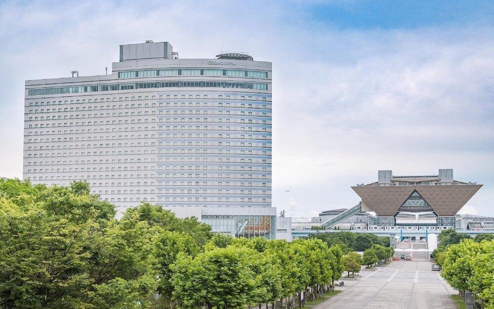
Tokyo Big Sight & Tokyo Bay Ariake Washington Hotel
Day 3 Forum & Reception: Dec 10, 5:30 - 7:00 PM (BNV Launch & Reception)
Delegation Size
50+ Representatives
Limited Capacity — Register Early
Indian Government & Industry
Central & state missions · Fabs & OSATs · Incentives · Market scale
Japanese Semiconductor Ecosystem
Equipment · Advanced materials · Technology transfer · JVs
STRATEGIC MISSION PILLARS
Four pillars driving the Japan–India semiconductor corridor
01
Semicon 2.0 Subsidies
Capital expenditure support of up to 40% under India’s INR 1.275 trillion Semicon 2.0 framework for fabs, OSATs and supply chains.
02
Japan-India Joint Ventures
Technology transfer, cleanroom infrastructure, compound semiconductor partnerships and equipment maintenance hubs.
03
Supply Chain Resilience
Connecting Indian manufacturers with Japan’s leading suppliers of chemicals, photoresists, silicon wafers and ultra-pure gases.
04
Venture & Deeptech Capital
The BNV-JIBB innovation partnership, connecting Japanese venture and institutional funds with India’s semiconductor leaders.
WHY WE ARE GOING
Purpose of the Delegation
The programme covers SEMICON, company meetings, the BNV-JIBB partnership launch, and engagements with Indian and Japanese government bodies, banks and industry associations, focusing on investment, technology transfer, market entry and supply chains, alongside networking and cultural visits.
Beyond the exhibition floor, the seven days connect Indian policy makers and semiconductor leaders with Japanese equipment makers, materials companies, venture funds and government stakeholders. Highlights include the Japan-India Semiconductor Forum 2026, the BNV partnership launch and a networking dinner at the Embassy of India.
Who should attend
- checkCentral & State Government Officials (Industry, Investment, Technology & Policy)
- checkIndian Semiconductor, Electronics & Advanced Manufacturing Companies
- checkSupply Chain Stakeholders (Equipment makers, materials suppliers & infrastructure providers)
- checkInstitutional Investors, Venture Capital Funds & Deeptech Start-ups
- checkTechnical Universities, Research Institutions & Scientists
- checkEstablished Business Houses seeking to enter or invest in semiconductors
7-DAY ITINERARY
7-Day Delegation Mission Itinerary
Departure
expand_more
- EveningDepart India on an overnight flight to Tokyo.
Outcome
Delegates begin the journey to Japan as scheduled.
SEMICON & Industry Engagement
expand_more
- 7:30–9:30 AMArrive in Tokyo; hotel transfer, check-in/breakfast and travel to Tokyo Big Sight for registration.
- 10:00 AM–12:30 PMSEMICON exhibition: semiconductor manufacturing and production.
- 12:30–1:30 PMLunch and networking.
- 1:30–3:30 PMOne-to-one company meetings on partnerships, technology and investment.
- 3:30–4:30 PMSEMI sessions on technology, manufacturing innovation and industry developments.
- 4:30–5:00 PMNetworking on industry insights and collaboration.
- EveningDinner and informal networking.
Expected outcome
Arrive at Japan’s semiconductor ecosystem; identify potential partners and suppliers; explore business and technology opportunities.
Seminar & Investor Engagement
expand_more
- 7:30 AM–12:30 PMBreakfast, SEMICON exhibition visits at Tokyo Big Sight and lunch; then transfer to Ariake.
- 1:30–5:00 PMJapan-India Semiconductor Forum 2026 (JIBB), Tokyo Bay Ariake Washington Hotel: India outlook, Semicon 2.0 incentives, investment and technology partnerships.
- 5:30–7:00 PMNetworking reception and business-card exchange; BNV Launch & Partnership Announcement with JIBB.
- EveningReturn to hotel; free evening.
Expected outcome
Understand Semicon 2.0 incentives; identify investment, innovation and technology partnerships; strengthen institutional cooperation.
Institutional Engagement & Embassy Dinner
expand_more
- 7:30–9:30 AMBreakfast and transfer to Tokyo Big Sight.
- 9:30 AM–1:30 PMExhibition visits, company meetings and relevant conference sessions.
- 1:30–3:00 PMLunch and informal networking.
- 3:00–4:30 PMReview India-Japan semiconductor cooperation and key findings.
- EveningNetworking dinner at the Embassy of India, Tokyo, with Embassy officials and Japanese industry representatives.
Expected outcome
Build business connections with Japanese companies, financial institutions and chambers; identify investment, manufacturing, technology and business opportunities.
Proposed Day Excursion (TBC)
expand_more
- 7:00–8:00 AMBreakfast at the hotel.
- To be confirmedProposed day excursion — destination and programme to be confirmed.
- EveningFree time or separately arranged dinner.
Outcome
Experience Japanese culture and strengthen informal networking among delegates.
Technology & Cultural Visit
expand_more
- 10:00 AM–2:00 PMBreakfast and guided tour of Asakusa, Senso-ji Temple, Shibuya Crossing and Odaiba.
- 2:00–3:00 PMLunch.
- 3:00–5:00 PMVisit Tokyo Skytree and either teamLab Planets or teamLab Borderless.
- 6:30–8:30 PMJapanese dinner and networking to reflect on the visit and India-Japan exchange.
Outcome
Exposure to Japanese innovation, cultural traditions and the wider business environment.
Return to India
expand_more
- 5:30–6:30 AMBreakfast and hotel check-out.
- 11:45 AM–6:20 PMDeparture from Japan and return to India.
- Per flightTransfer to Haneda or Narita.
Outcome
Delegates return to India with key insights, connections and next steps for India-Japan collaboration.
Timings and engagements are subject to confirmation.
DAY 3 FOCUS
Japan-India Semiconductor Forum
Date & Time
Thu, 10 Dec 2026, 1:30–5:00 PM
Registration opens 1:00 PM
Venue
Tokyo Bay Ariake Washington Hotel
3F Conference Room "Iris", Ariake, Koto-ku
Organiser
Japan-India Business Bureau (JIBB)
Access & Language
Free; first 200 attendees
Japanese & English, consecutive interpretation
Why it matters: Semicon 2.0
In July 2026 the Government of India approved Semicon 2.0, the second phase of its semiconductor support programme. Support now extends to manufacturing equipment, materials, chemicals and gases, fields where Japanese companies are strong. The forum covers India’s investment and subsidy policy and the initiatives of key Indian and Japanese players.
Source: Press Information Bureau (PIB), India Semiconductor Mission
celebrationNetworking reception · 5:30–7:00 PM
Reception and business-card exchange, free of charge, limited to the first 80 attendees. Register delegates early. The BNV Launch & Partnership Announcement with JIBB is proposed for this window (slot to be agreed with JIBB).
flagSEMICON India 2028 Japan Pavilion
Call for exhibitors is open; show scheduled for March 2028. The forum will present the Pavilion outline and the exhibitor invitation.
domainNoida permanent exhibition centre
SEMICON India is not held in FY2027, so use the centre near Delhi. Year-round promotion with concierge, monthly networking events, plus market research, consulting, JV and key-person identification, company set-up, materials purchasing and distribution.
RATIONALE
Purpose & Rationale
Engage with Japanese industry, investors and institutions to explore collaboration and strengthen India-Japan partnerships in semiconductors and advanced technologies.
India’s Opportunity
- trending_upGrowing semiconductor market
- trending_upExpanding manufacturing capabilities
- trending_upGovernment support to attract investment
Japan’s Strengths
- verifiedLeadership in materials and equipment
- verifiedAdvanced technology and innovation
- verifiedStrong industry base and financial institutions
Objectives
- 01Identify potential Japanese technology partners, equipment manufacturers and supply-chain collaborators.
- 02Explore investment, technology and commercial collaboration opportunities.
- 03Facilitate engagement with Japanese companies, investors, research institutions and innovation stakeholders.
- 04Understand developments in semiconductor manufacturing, materials, inspection, and advanced packaging.
- 05Define follow-up actions for participating Indian government and industry stakeholders.
WHAT YOU TAKE HOME
Key Delegation Deliverables & Takeaways
1. Engagement Record
Comprehensive record of meetings, organizations met and key discussion points
2. Opportunity Tracker
Potential business, technology and investment opportunities with next steps
3. Follow-up Plan
Actions, responsible persons and timelines for follow-up
4. Delegation Report
Summary of visits, key findings and recommended next steps
5. India-Japan Pipeline
Promising opportunities for further discussion, subject to review and agreement by both parties
LOGISTICS & FUNDING
What the Delegation Package Covers
Return international flights
Coordinated schedules from major Indian hubs to Tokyo (Haneda/Narita) and back.
Tokyo accommodation
5-star hotel accommodation in Tokyo for 6 nights (hotel to be confirmed).
Meals incl. vegetarian & Jain
Meals throughout, including Indian catering, vegetarian and Jain preparations.
Ground transport
Dedicated coaches for airport transfers, Big Sight, Embassy events and excursions.
SEMICON passes
Exhibition passes, conference credentials and badge coordination.
Bilingual support
Japanese-English interpreters for one-to-one business meetings, plus visas and insurance.
HOW PAYMENT WORKS
End-to-end travel management
Within the confirmed scope, JIBB coordinates airfare, accommodation, meals, local transport, excursions, cultural visits, visas, insurance, interpretation and related services.
Single up-front payment
Each delegate pays the applicable package cost to JIBB in one consolidated payment before travel, for timely bookings and smooth service.
WHO DOES WHAT
Roles & Responsibilities
JIBB
Coordinate Japanese stakeholder engagement and meeting requests; manage programme, delegate information and follow-up documentation, subject to agreed scope and resources.
Delegation Participants
Attend scheduled engagements, comply with travel and event requirements and provide timely inputs for follow-up reporting.
Japanese Hosts & Partners
Confirm meetings, venue access and participating representatives; facilitate host-specific requirements.
Travel & Logistics Provider
Coordinate flights, accommodation, ground transport, insurance and services; provide on-ground support.
JOIN THE DELEGATION
Register for the Delegation
Scan the QR code with your phone camera or open the registration form below. For any questions, contact the delegation coordinator directly.

Scan to register
Address
Tokyo Big Sight & Tokyo Bay Ariake Washington Hotel
Ariake, Koto-ku, Tokyo 135-0063, Japan
Open in Google Mapsarrow_forwardTransit & Access
Yurikamome Line (Tokyo Big Sight Station ~3 min walk)
Rinkai Line (Kokusai-Tenjijo Station ~7 min walk)
From Airports
~25 min via Airport Limousine Bus from Haneda Airport (HND)
~60 min from Narita (NRT)
Convention Center Guide
Tokyo Big Sight & Tokyo Bay Ariake Washington Hotel, Ariake, Tokyo