
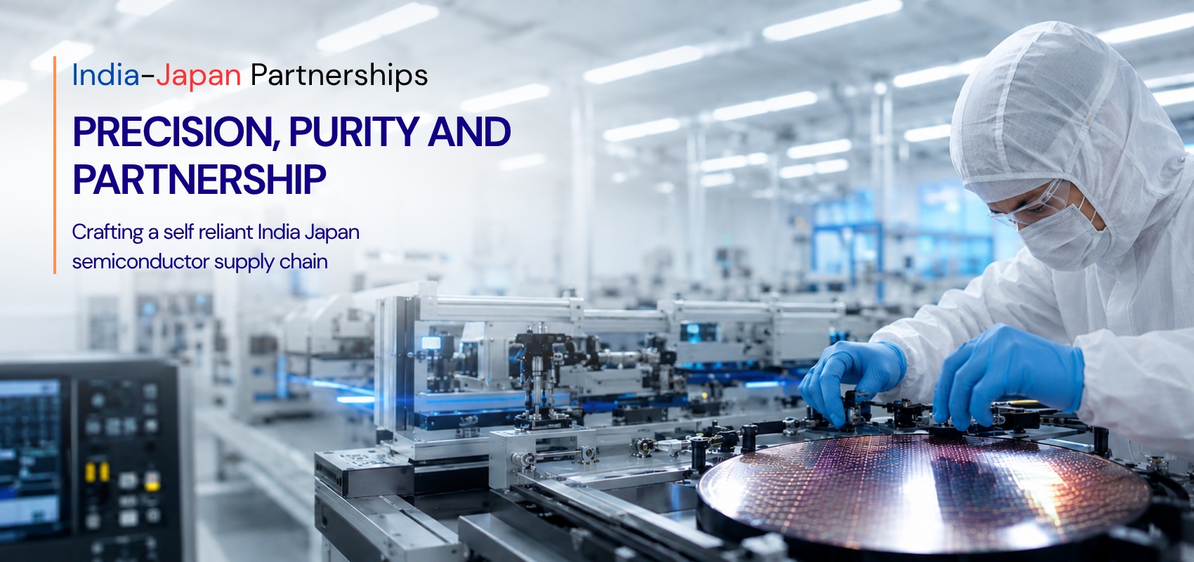
India's semiconductor ambition is often measured in fabs and subsidies — headline numbers of billions of dollars and millions of chips per day. That is the visible tip. Beneath it lies a far more intricate story: the story of chemicals so pure they are measured in parts per trillion, of lithography equipment that aligns features to fractions of a nanometre, of packaging materials that dissipate heat while withstanding extreme thermal cycling, and of a design ecosystem that increasingly scripts the architecture of global artificial intelligence, automotive, and communications systems. It is in this granular, deeply technical layer that the India‑Japan partnership discovers its most compelling logic.
The Materials Kingdom: Japan's Invisible Crown
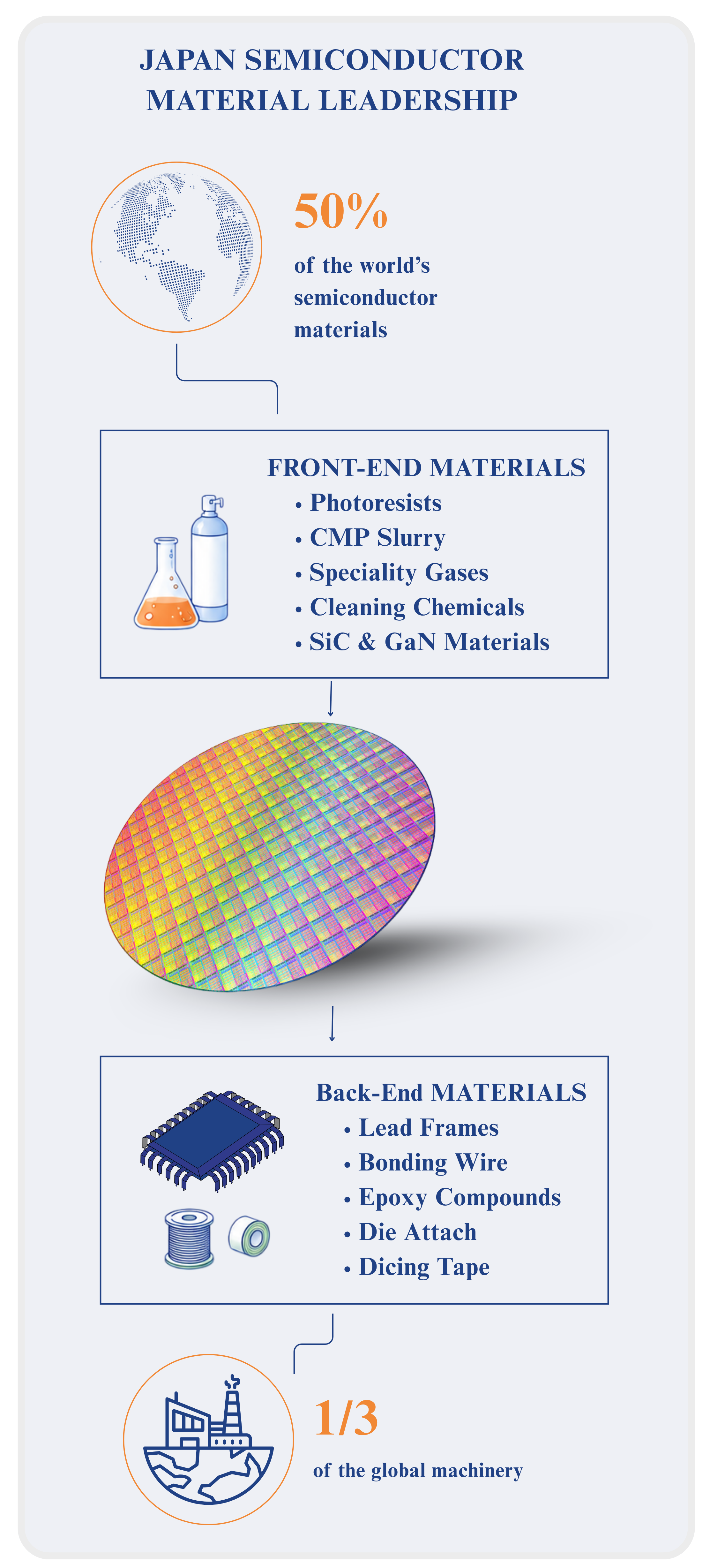 Figure 1: Japan's dominant share in global semiconductor materials supply.
Japan supplies roughly 50% of the world's semiconductor materials and one‑third of the global machinery. This dominance is not accidental; it is the product of decades of cumulative processing know‑how. Consider the value chain for the front‑end fabrication process. To pattern circuits on a silicon wafer, one needs photoresists that are sensitive yet stable — Japan's Shin‑Etsu Chemical and JSR control the lion's share of the ArF, KrF, and EUV resist markets. Planarisation demands CMP slurry; Japanese firms including Fujimi and Hitachi Chemical are global benchmarks. Thin‑film deposition and etching require a cocktail of specialty gases — WF₆, SiH₄, HBr, CF₄ — where the purity levels must be so exacting that a single stray molecule can destroy a wafer batch. Japan's Taiyo Nippon Sanso and Air Water master this chemistry. Ultra‑high‑purity cleaning agents, such as hydrogen peroxide, aqueous ammonia, and sulphuric acid with ppq‑level impurity control, are the province of firms like Sumitomo Chemical and Mitsubishi Chemical. In compound semiconductors, Japan leads in SiC and GaN substrates, epitaxial layers, and crystalline materials crucial for electric‑vehicle power devices.
The back‑end, too, is a Japanese‑engineered world. Lead frames made from Cu/Fe‑Ni alloys, epoxy moulding compounds that encapsulate chips, bonding wire of gold, copper, and silver, die‑attach solders and silver pastes, dicing tape, solder balls for BGA applications — Japanese companies dominate every category.
From Lab to Fab: The Chemical Pivot to India
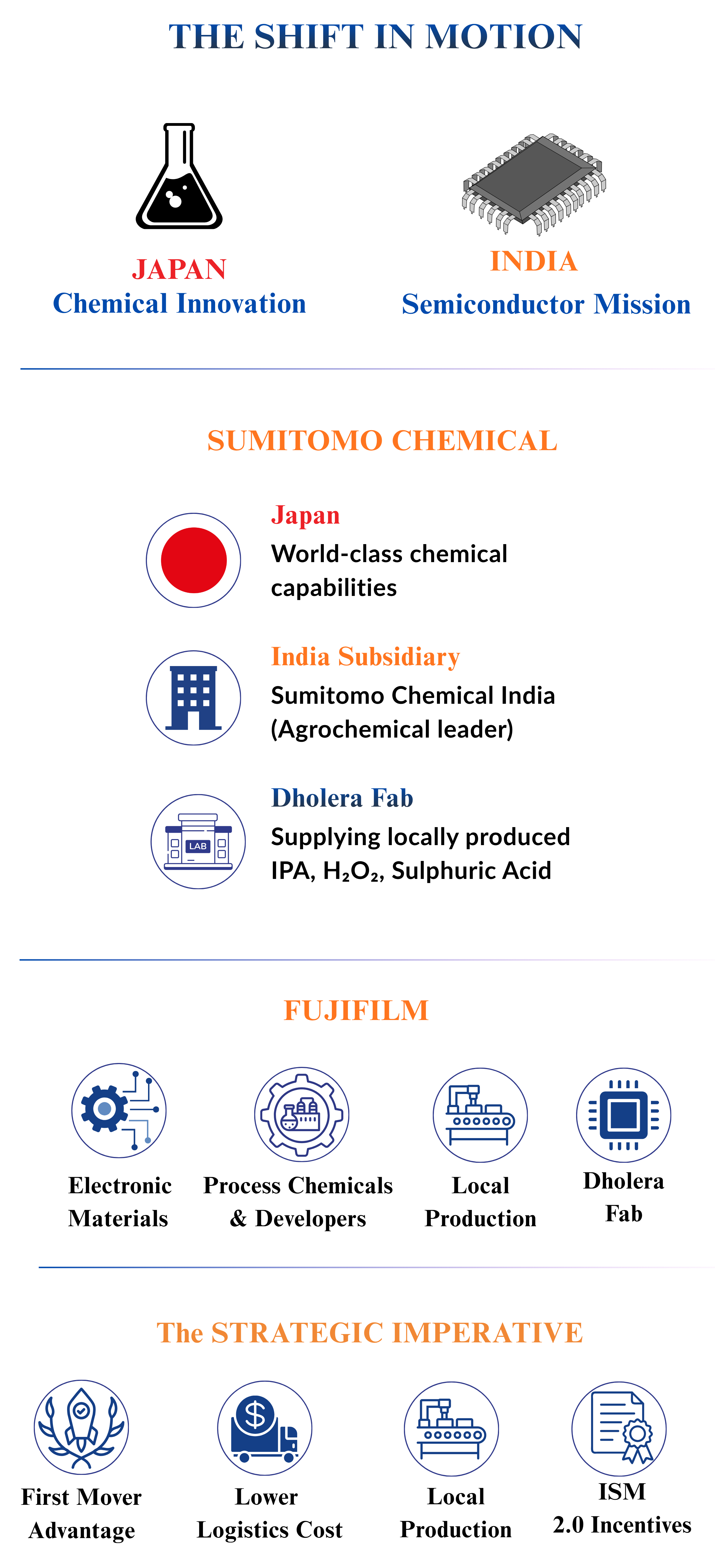 Figure 2: Shift of Japanese chemical investments to India.
The technical narrative is now acquiring a geography. In February 2026, Chemical & Engineering News documented a systematic shift: Japanese chemical firms are slowing investments in China and accelerating them in India. The drivers are not just geopolitical but also industrial. India's semiconductor policy demands domestic production of chips, which in turn demands local availability of high‑purity chemicals to reduce logistics cost, supply‑chain risk, and qualify for the fiscal incentives that ISM 2.0 now explicitly extends to materials manufacturing.
Sumitomo Chemical's journey is emblematic. The company operates world‑class semiconductor‑grade chemical plants in Japan, South Korea, China, and most recently Baytown, Texas. For India, it is aiming to supply Tata's Dholera fab with locally produced, ultra‑high‑purity isopropyl alcohol, hydrogen peroxide, and sulphuric acid. Critically, Sumitomo already has a substantial Indian presence through its listed subsidiary Sumitomo Chemical India, an agrochemical leader. The plan is to leverage that subsidiary's land, infrastructure, and regulatory familiarity to co‑locate semiconductor material facilities — a model that drastically shortens time‑to‑production and reduces capital outlay. General Manager Yasuo Yoshino frames it simply: "With the idea that the first mover captures the largest share, we aim to localise production."
Fujifilm's Electronic Materials Division is following a parallel track. With products spanning nearly all semiconductor process steps, Fujifilm sees the Dholera project as an anchor client that justifies local production. Senior Manager Tomoki Nakatani says the firm will "begin local production of process chemicals and developers, which incur high transportation costs." The logic is both commercial and technical: certain process chemicals degrade or become economically unviable during prolonged transport, making local manufacturing a prerequisite for any serious node.
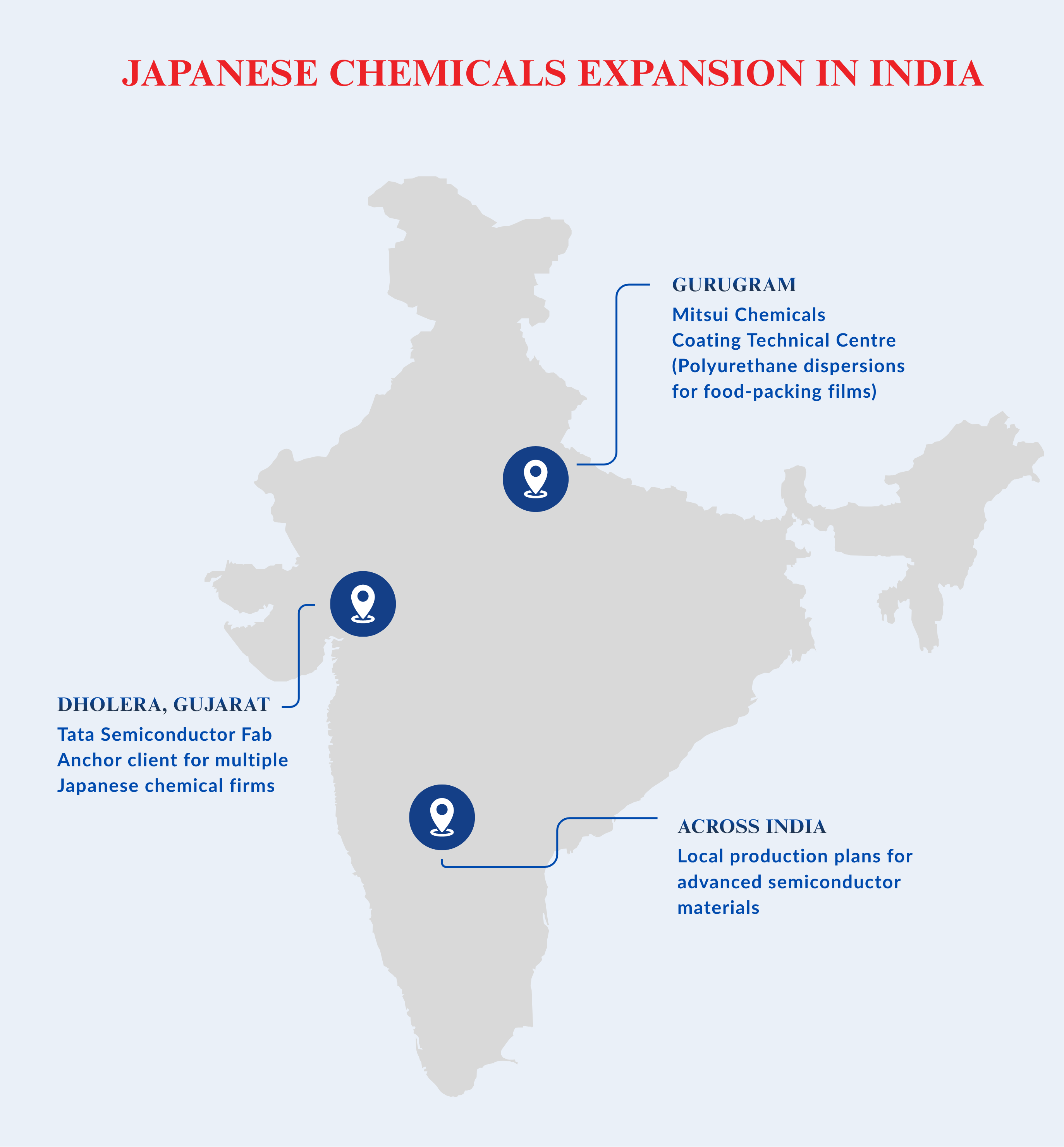
Mitsui Chemicals is evaluating local manufacturing of Tafmer polyolefin elastomers — the encapsulant material for solar panels — and EPDM rubber for automotive applications. Managing Director Jun Kawaguchi has linked this directly to India's solar‑panel localisation drive and EV growth, noting that solar panel production "has relied heavily on imports from China," and that EPDM demand will be propelled by automotive expansion. The company has also opened a coating technical centre in Gurugram to develop polyurethane dispersions for recyclable food‑packaging films, with full formulation capabilities targeted by 2027. Meanwhile, Mitsubishi Chemical, the largest Japanese chemical maker, is in the initial stage of considering local MMA production. CEO Manabu Chikumoto has publicly acknowledged that while the Indian MMA market is still small, a local presence renders it "resistant to external pressure."
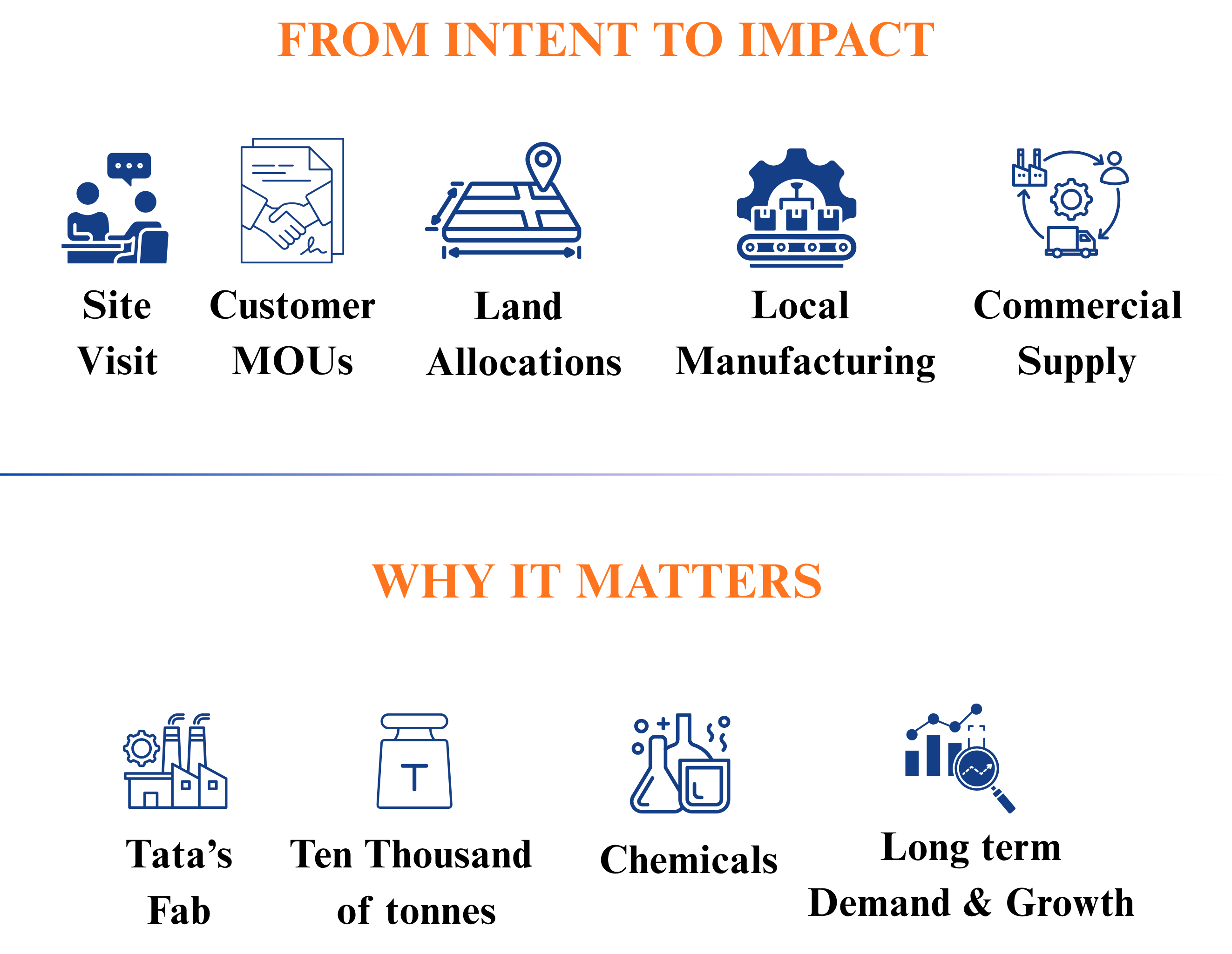
These are not speculative boardroom ideas. They are mature feasibility studies backed by site visits, customer MOUs, and in some cases, land allocations. The common thread is the pursuit of "first‑mover advantage" in a market where the anchor customer — Tata's fab — will need tens of thousands of tonnes of specialist chemicals annually once it reaches nameplate capacity.
The Equipment Equation: Precision at Scale
If materials are the bloodstream of a chip, equipment is its skeleton. Japanese semiconductor equipment makers, led by Tokyo Electron and SCREEN, command a significant share of the global etch, deposition, cleaning, and test markets. Tokyo Electron's MOU with Tata Electronics for equipment supply to the Dholera fab is a foundational step. It goes beyond machinery sales: the arrangement includes technical training, service infrastructure, and adaptation of equipment configurations to India's specific operating environment. When Prime Minister Modi visited TEL Miyagi in Sendai during his August 2025 Japan trip, he saw first‑hand the advanced manufacturing floor that similar Indian facilities will aim to replicate within a decade.
The ecosystem is thickening. Lam Research, though a US company, has committed over $1 billion in India for tool engineering, training programmes, and ecosystem development, signalling that global equipment firms view India as more than a sales market — they see a collaboration hub. SCREEN and TEL's presence, combined with ASML's local support systems being established, means that the equipment supply chain is gradually embedding in Indian soil. For Japan, this opens the possibility of component‑level manufacturing: the precision valves, seals, vacuum chambers, and controllers that go into semiconductor equipment are often fabricated by Japanese small‑ and medium‑sized enterprises. ISM 2.0's inclusion of "semiconductor equipment manufacturing" as a focus area is a direct invitation to these firms.
Innovation‑Led Design: Where Japan's Needs Meet India's Talent
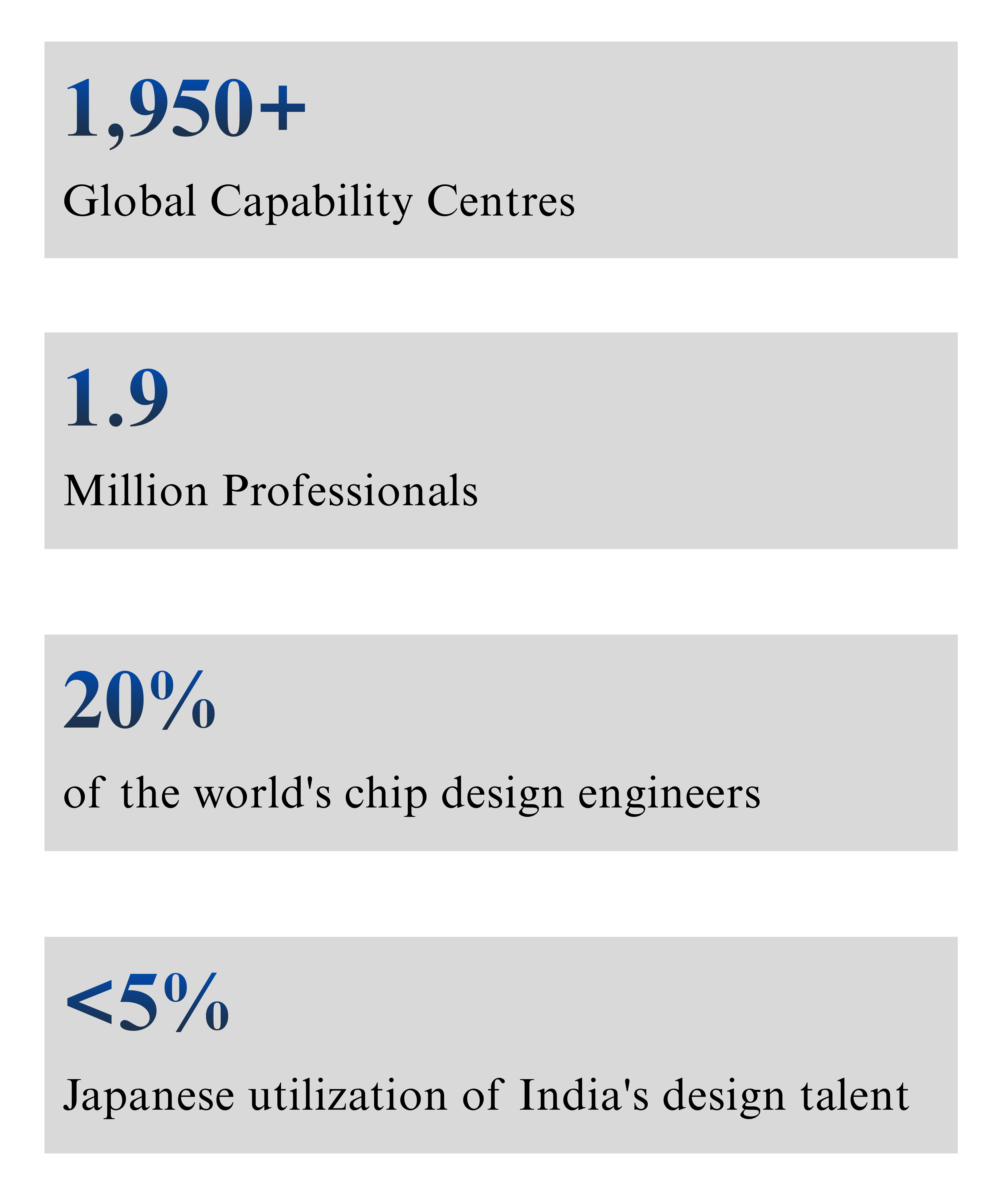 Figure 3: Matching Japan's talent needs with India's design capacity.
India's semiconductor design strength is no longer an abstract number. With 1,950 global capability centres employing over 1.9 million professionals, India accounts for approximately 20% of the world's chip design engineers, forming a major pillar of the India–Japan Semiconductor Partnership. Nearly every major global semiconductor company now runs a significant design operation in India — Qualcomm's 17,000‑strong team works on 5G modems, SoCs, and automotive platforms; AMD is doubling its headcount to 10,000 by 2028; NVIDIA, Micron, and Texas Instruments each have thousands of engineers developing AI chips, memory architectures, and verification solutions. For Japan, the picture reveals a yawning gap: Japanese companies currently utilise less than 5% of the design talent active in India.
That is changing quickly. Renesas Electronics has established a 3 nm design centre in India, directly feeding its automotive system‑on‑chip ambitions. ROHM is expanding power and analog LSI design teams. Sony leverages Indian image‑sensor design for AI and surveillance applications. The Design Linked Incentive (DLI) scheme has catalysed 23 indigenous projects covering video‑analytics SoCs, satellite‑compatible NB‑IoT chips, SiC‑based power controllers, and RISC‑V multicore processors for edge AI. India's Ministry of Electronics and IT, together with academic institutions like the IITs and IISc, is training 100,000 semiconductor engineers — a number that directly addresses Japan's projected shortfall of 790,000 advanced‑technology workers by 2030. The talent arbitrage is transforming into a co‑creation model: Japanese companies set the product specification and system‑level reliability targets, while Indian teams execute the design, verification, and software stacks. The result is a shorter time‑to‑market for EV power modules, automotive radar chips, and industrial IoT nodes — all sectors where demand in both India and Japan is surging.
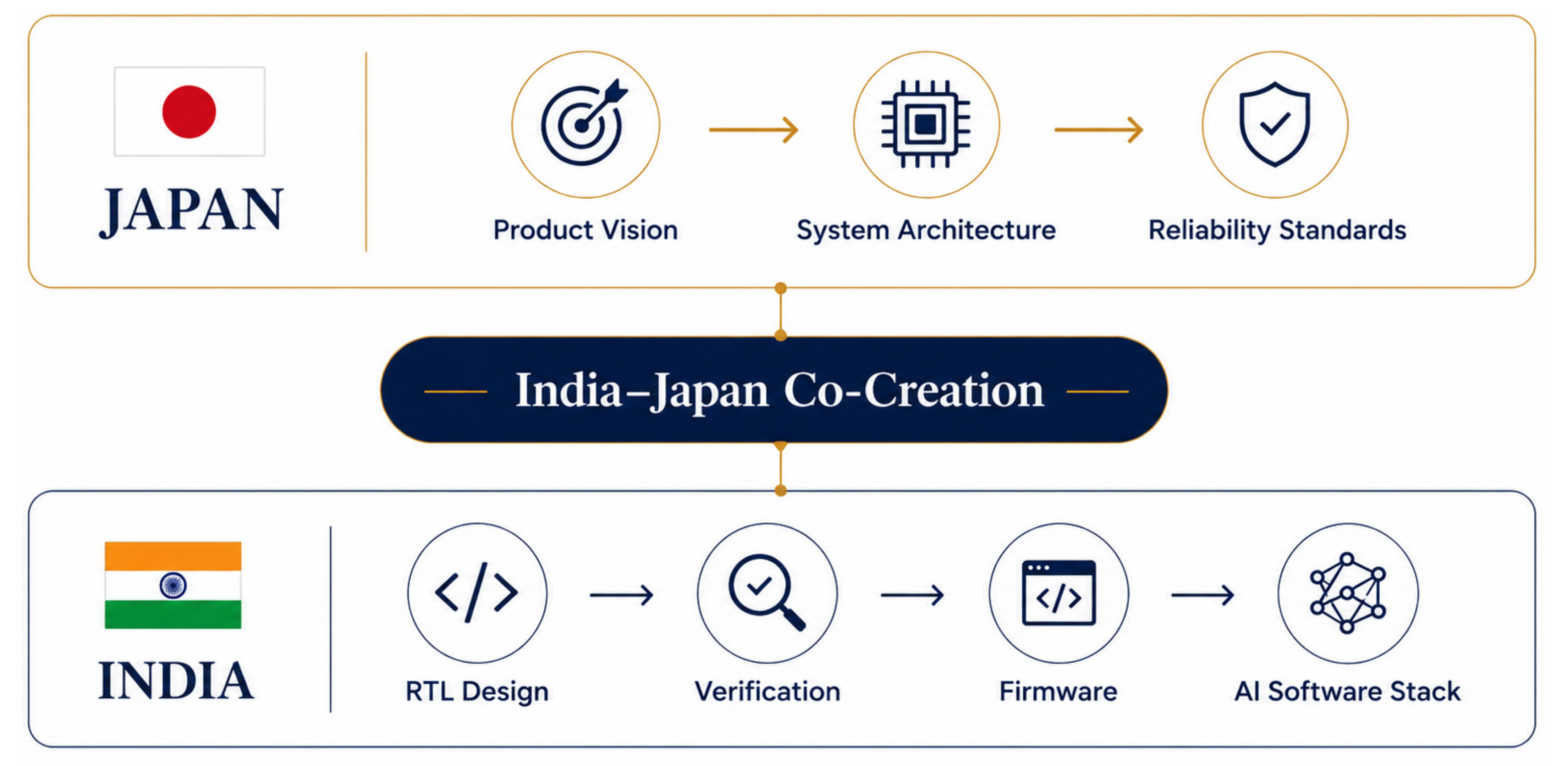 The co-creation model between Japanese system specs and Indian engineering execution.
The Back‑End as India's Competitive Theatre
Back‑end semiconductor processes — assembly, testing, marking, and packaging — are considerably more labour‑intensive than front‑end fab operations. This structural fact aligns with India's demographic profile. The OSAT facilities in Sanand are already demonstrating productivity metrics that justify the model. Kaynes Semicon's plant targets six million chips per day. The Tata Assam OSAT will handle the output of the Dholera fab. CG Power's Renesas‑backed unit adds a critical pillar: packaged chips for automotive, industrial, and IoT markets.
India's cost‑competitive workforce, combined with the progressive automation that Japanese firms like DISCO (dicing saws) and Advantest (test systems) supply, creates a hybrid model — labour‑assisted precision — that can deliver price and quality simultaneously. Over time, as the Dholera fab matures and more front‑end capacity is announced, the back‑end cluster in Gujarat, Assam, and Odisha will be able to serve not only Indian fab output but also imported wafers from Japan, Taiwan, and Singapore for final packaging, testing, and shipment. This is the vision of India as a global packaging hub, not merely a captive domestic supplier.
Export Opportunities and Atmanirbhar Bharat
Fujifilm's CEO Teiichi Goto has crystallised the export logic: India's significance "will grow not only as a market in itself but also as a supply base for the Middle East, Africa, and neighbouring Asian countries." The India‑EU Free Trade Agreement, concluded in January 2026, removes tariffs on over 96% of goods and opens a continental market for products manufactured in India. Japanese suppliers setting up in India can, using the EU FTA's rules of origin, export high‑value semiconductor sub‑assemblies and materials to Europe duty‑free. The same applies to markets in ASEAN and Africa, where India's geographical position and improving logistics (the dedicated freight corridors, the upcoming SEZ‑linked container depots) offer a freight‑cost advantage over East Asian competitors.
Atmanirbhar Bharat — self‑reliant India — is not about autarky. It is about creating a manufacturing ecosystem where the most demanding inputs — advanced substrates, photoresists, clean‑room chemicals, vacuum components, packaging resins — are produced locally, thereby shielding the economy from the kind of supply‑chain bottlenecks that crippled industries during the pandemic and that are now being repeated through the Hormuz disruption. By partnering with Japan, India can internalise the technologies it currently imports while simultaneously offering Japanese firms a lower‑cost, high‑growth manufacturing base that is politically and economically aligned. Facilitating this transition is where organisations like the Japan India Business Bureau (JIBB) provide active, hands-on support in partner identification and site advisory.
Resilience and the China‑Plus‑One Calculus
The most powerful subplot is the China factor. The Chemical & Engineering News report catalogues a series of Japanese divestments from China: DIC exiting LCD materials, Sanyo Chemical selling its superabsorbent polymer subsidiary, Sumitomo Chemical divesting polypropylene and LCD polariser units, Mitsui Chemicals transferring its phenol JV stake, Kuraray selling its acrylic‑sheet subsidiary. Japan's overall investment in China was down 46% year‑on‑year in 2024. In parallel, India has enacted technology‑leakage protection legislation modelled on Japan's own laws, directly addressing the intellectual‑property concerns that have long deterred high‑tech Japanese investment. This is a comprehensive risk‑hedge framework: a friendly jurisdiction with strong IP protection, rising incomes, and virtually insatiable demand for electronic goods.
The Precision‑Purity‑Partnership Trinity
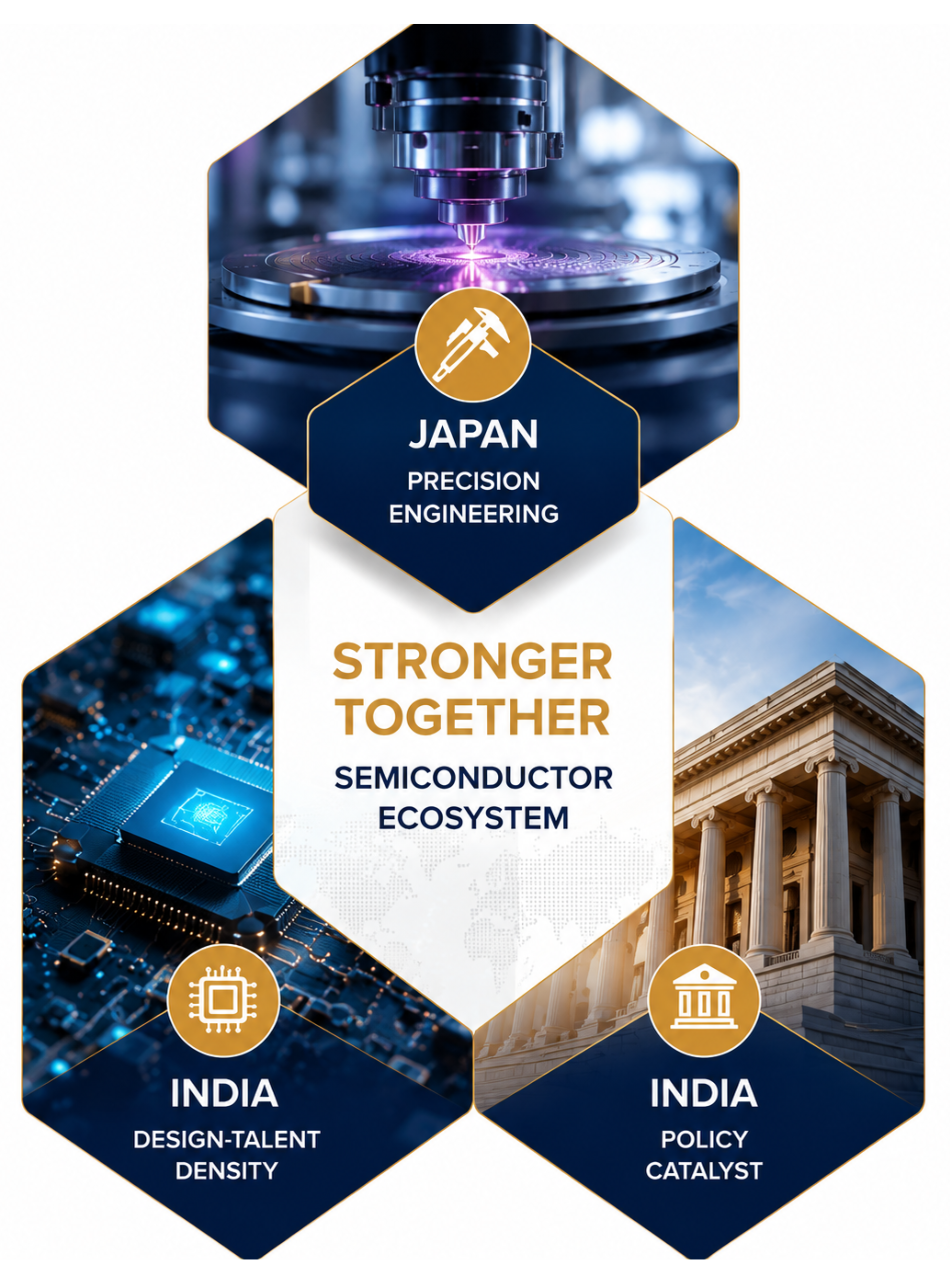 Figure 4: The three-way synergy between Japanese technology, Indian talent, and policy incentives.
Japan's precision engineering, India's design‑talent density, and the catalytic effect of Indian policy together form a trinity that is more resilient than any single‑country strategy. The chemistry is literal and figurative: high‑purity Japanese chemicals will wash the wafers produced in Dholera; Japanese lithography coater‑developers and photoresists will pattern the transistors; Indian‑designed chips will power EVs across Asia; Indian‑packaged modules will find their way into European factories. In every link of this chain, the technologies and business models of both nations complement rather than compete.
For Indian enterprises, the path is clear: partner with Japanese materials and equipment makers to leapfrog the learning curve, participate in the DLI programme to monetise design IP, and leverage the state‑stacked incentive regimes to build capital‑intensive production lines. For Japanese firms, the imperative is equally sharp: deploy materials manufacturing capacity in India now, lock in long‑term supply contracts with anchor customers like Tata and Micron, and access India's overflowing engineering pipeline to sustain innovation at home. This is not a transaction; it is a structural integration of two technology ecosystems that, together, can serve as the backbone of a self‑reliant, export‑oriented semiconductor supply chain for the Indo‑Pacific century.