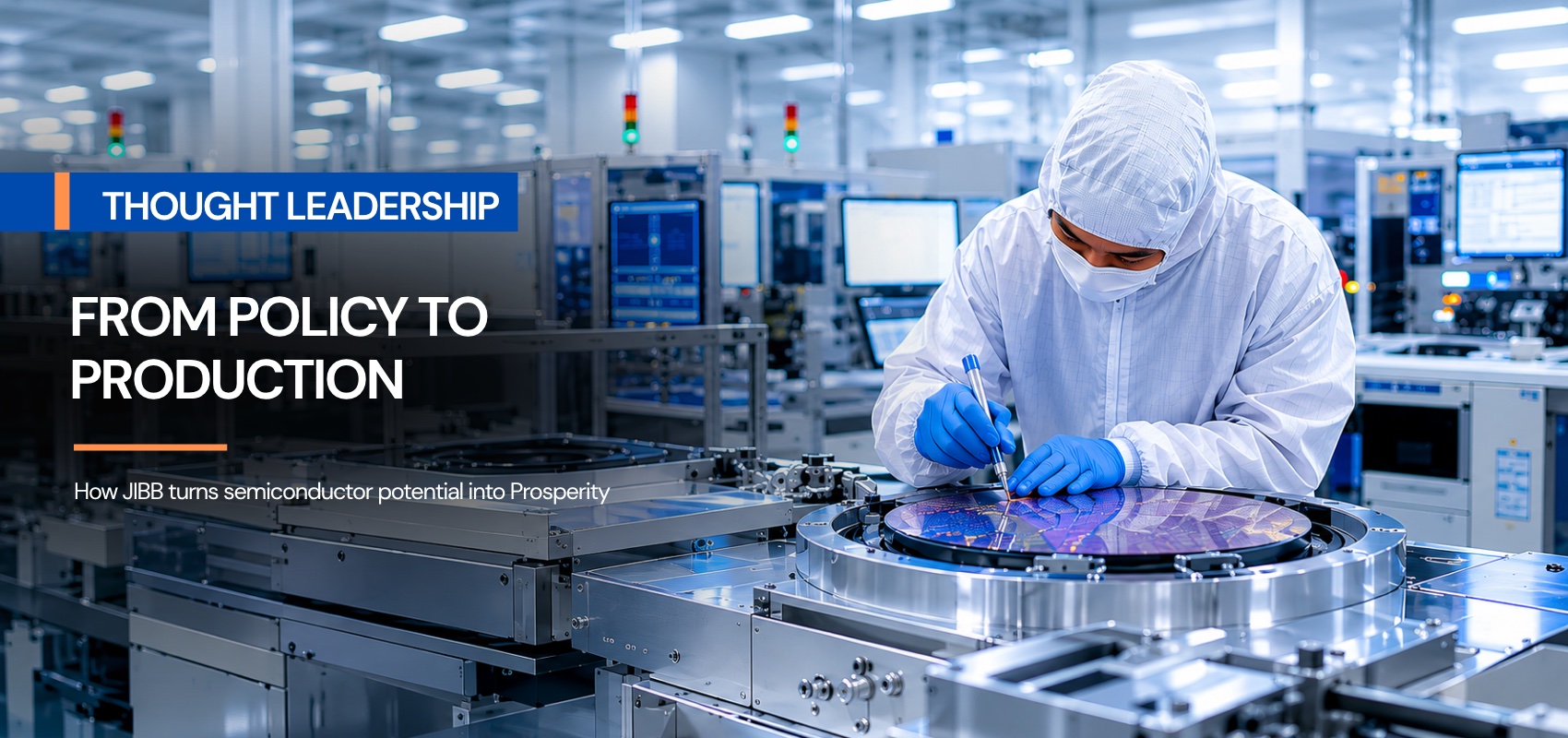
The India–Japan semiconductor corridor has all the ingredients of a transformative partnership—world-class Japanese materials and equipment, a massive and policy-supported Indian market, a growing design-talent pool, and high-level political alignment.
Yet, as External Affairs Minister S. Jaishankar noted in March 2026, “trade figures still fall below expectations.” The gap between strategic potential and commercial delivery is where the Japan India Business Bureau (JIBB) operates.
Our mission is to be the institutional bridge that converts frameworks into factories, MOUs into operating revenue, and individual projects into an integrated, resilient ecosystem.
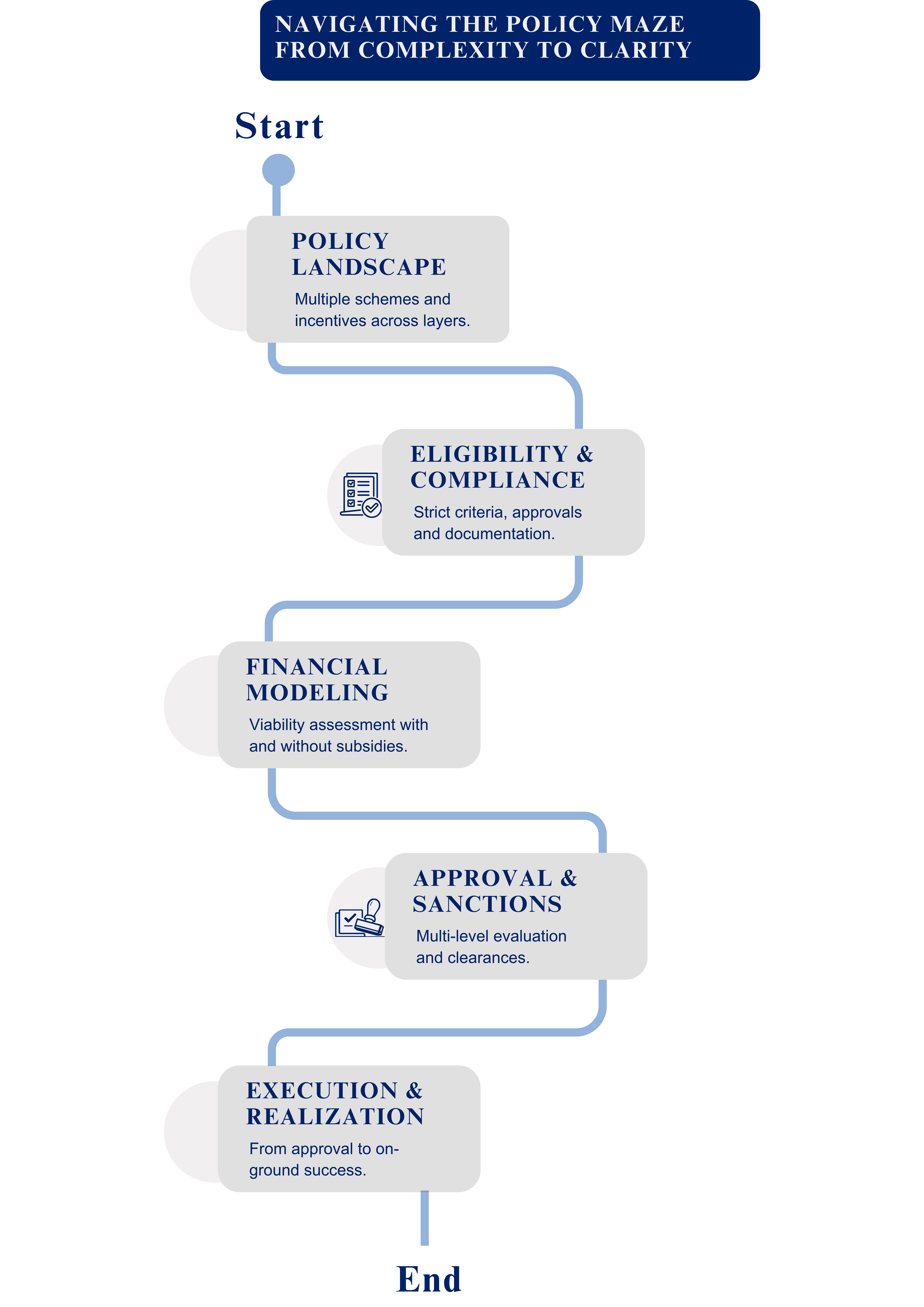
Navigating the Policy Labyrinth: ISM 2.0 and Beyond
Figure 1: Navigating the India semiconductor policy layers.
India’s semiconductor incentive architecture, while generous, is complex. A typical Japanese mid-sized firm—a Chuken company—evaluating a materials plant must contend with multiple layers of fiscal support.
The central government provides:
- Up to 50% capital expenditure support for ATMP/OSAT and compound-semiconductor projects.
- A Design-Linked Incentive (DLI) covering up to 50% of design costs.
- New equipment and materials support under the India Semiconductor Mission 2.0.
State governments further enhance support through:
- Capital subsidies
- Stamp-duty waivers
- SGST reimbursements
- Training assistance
For example, Gujarat’s semiconductor policy can increase effective project-cost coverage to 70% when combined with central incentives.
How JIBB Helps
JIBB’s policy-advisory practice helps companies navigate this landscape by:
- Preparing detailed feasibility studies aligned with ISM subsidy requirements.
- Verifying eligibility criteria related to investment size, revenue history, and corporate structure.
- Ensuring proposals include credible technology-upgrade roadmaps and customer tie-up plans.
- Stress-testing financial models without subsidies so clients understand core project economics before layering incentives.
We also guide companies through environmental, land, water, and labour approvals required for subsidy disbursement, leveraging the National Single Window System and state-level clearance interfaces.
SEZ Support
For Japanese companies unfamiliar with India’s SEZ reforms, JIBB provides end-to-end site-selection support.
The June 2025 SEZ rule changes:
- Reduced minimum land requirements to 10 hectares
- Allowed free-of-cost inputs to count toward NFE
- Permitted domestic sales upon duty payment
These reforms have unlocked previously unviable projects.
The Tata Semiconductor SEZ notification of April 2026 marked a major milestone in regulatory coordination. JIBB is currently working with several Japanese chemical and gas suppliers to evaluate SEZ-eligible sites in Gujarat, Uttar Pradesh, and Odisha. This ensures logistics models capitalize on inland container depots, dedicated freight corridors, and proximity to anchor fabs.
Partner Identification: Chuken-to-Chuken and Beyond
Successful semiconductor investment requires more than incentives—it requires the right partners. JIBB helps Japanese and Indian mid-sized enterprises identify complementary collaborators across the semiconductor value chain.
Our support includes:
- Market-entry assessments
- Partner screening and qualification
- Commercial matchmaking
- Strategic alliance development
- Cross-border business facilitation
By combining sector expertise with extensive industry networks, JIBB accelerates the formation of durable business relationships that can scale into long-term industrial partnerships.
Building Consortia and Supply-Chain Clusters
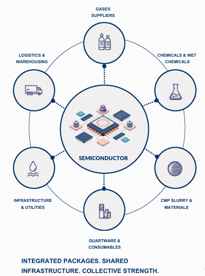
Figure 2: Supplier clusters and industrial ecosystem coordination.
Semiconductor manufacturing is a collective enterprise. Tata’s Dholera fab alone will eventually consume thousands of tonnes of chemicals, gases, and substrates annually, requiring a ring of suppliers located within a 30-minute radius to ensure just-in-time delivery of ultra-high-purity materials. This co-production strategy aligns with the broader India-Japan manufacturing partnership focusing on supply-chain resilience.
JIBB actively forms supplier consortia that can offer integrated packages. For example, a consortium may include companies specializing in high-purity gases, wet chemicals, CMP slurry, photoresist strippers, and quartzware. These groups can jointly negotiate with anchor customers and share infrastructure such as gas pipelines, deionised water plants, and hazardous-waste treatment facilities.
Structured Delegations
JIBB organizes and leads structured delegations modeled on the visit of 20 Japanese semiconductor ecosystem companies to Dholera following SEMICON India 2025. These are not generic trade missions.
Each visit is preceded by a technical matching exercise that maps the production inputs required by Indian anchor projects, including wafer-cleaning agents, encapsulation resins, and test-handling equipment. JIBB then recruits Japanese firms best positioned to supply those requirements.
During these visits, participants:
- Tour active construction sites
- Meet procurement teams from Tata and Micron
- Engage with state industrial development corporations
Talent, Training, and the Workforce Bridge
Japan’s demographic constraints are well documented. The country anticipates a shortage of 790,000 advanced-technology workers by 2030. India, by contrast, produces approximately 1.5 million engineering graduates annually and has a national plan to train 100,000 semiconductor-specific engineers. Furthermore, 25,000 specialized professionals have already moved to Japan over the last five years for work, study, or training.
JIBB views this as a bidirectional talent pipeline.
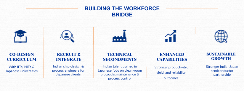
Bicultural training and workforce integration.
Curriculum Development
We collaborate with IITs, NITs, and Japanese universities to co-design curricula focused on:
- Semiconductor process engineering
- Materials science
- Industrial automation
Recruitment Support
For Japanese clients, we facilitate recruitment of Indian chip-design and process engineers. This is not merely a cost-arbitrage strategy. It is an innovation strategy that injects India’s scale of talent into Japan’s product-development cycles.
Technical Secondments
For Indian clients, we arrange technical secondments to Japanese factories, enabling operators and technicians to learn clean-room protocols, equipment maintenance practices, and statistical process control methodologies. This human-capital layer is often overlooked in investment promotion, yet it remains the single most critical factor in achieving yield and reliability targets.
The Road Ahead: Closing the Trade Gap
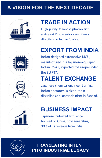
Figure 3: JIBB's vision for 2030.
JIBB’s vision is that by the end of this decade, the India–Japan semiconductor partnership will be visible not only in government communiqués but in daily commercial reality:
- High-purity Japanese-produced photoresist arriving at Dholera and being piped directly into fabrication facilities.
- Indian-designed automotive MCUs manufactured in Japanese-equipped Indian OSAT facilities and exported to European automakers under the EU FTA framework.
- Japanese chemical engineers training Indian operators in clean-room discipline at materials plants in Sanand.
- Japanese mid-sized firms that once focused primarily on China generating significant revenue from Indian subsidiaries.
The frameworks already exist: ISM 2.0, the renewed CEPA, the Dedicated India Office within Japan’s Ministry of Foreign Affairs, and Japan’s ¥10 trillion investment target. The counterparties are mobilizing: component manufacturers, global chemical groups, and equipment-technology leaders.
What the ecosystem needs is a translator of intent into action, a navigator through regulatory complexity, and a convener of complementary capabilities.
The Japan India Business Bureau is precisely that.
We invite Japanese and Indian companies to engage with us to transform the semiconductor moment into a multi-generational industrial legacy.